gesponsertSecond sourcing in power semiconductorsA second MOSFET is not yet an alternative
5 min Lesedauer
Fetek wants to establish itself in Europe as an application-driven silicon power MOSFET supplier and second-source partner for power semiconductor applications. Rather than focusing on record-breaking specifications, the company emphasizes a practical balance between efficiency, thermal performance, packaging, supply stability and cost competitiveness.
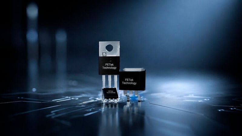
Fetek offers power MOSFETs in different package formats. For a suitable second source, however, mechanical and electrical similarity alone is not enough – what matters is how the device behaves in the actual design.
(Bild: Fetek)
When a MOSFET has to be replaced, the search often starts with a few familiar values: blocking voltage, current, RDS(on) and package. If another device with similar specifications is available, the solution may initially look straightforward. The data sheet alone, however, does not determine whether the new device is a real alternative.
Gate charge, capacitances, switching behavior, thermal characteristics and safe operating area may all differ. Two devices can look similar on paper and still behave differently in an existing design. And even a technically suitable MOSFET is of little use if the new supplier cannot deliver a few months later.
This is where Fetek is trying to position itself. According to the Taiwanese fabless company, its current focus is mainly on silicon power MOSFETs. What stands out is less a single technical record than the way Fetek describes its development target. The aim is not simply to push RDS(on) lower or switching speed higher, but to achieve a workable balance between efficiency, thermal behavior, packaging, supply and cost.
That sounds less spectacular than many semiconductor roadmaps. In a real design, it may matter more.
The best single value is not enough
According to Fetek, current development is focused primarily on low- and medium-voltage MOSFETs based on shielded-gate-trench technology. The latest generations are intended to combine lower conduction losses with improved switching behavior, better thermal performance and a wider safe operating area.
Low RDS(on) remains important because it reduces losses in the conducting state. In a fast-switching converter, however, it is not the only relevant value. Gate charge and the dynamic behavior of the transistor also affect losses. Depending on the application, an improvement in one area can therefore be partly offset by a disadvantage elsewhere.
Fetek describes this balance as one of its main development targets. Detailed device-level comparisons depend strongly on the target application, operating conditions and design requirements. The written answers do not include a specific before-and-after data set, so for engineers the real evaluation begins with the actual device – including RDS(on), gate charge, switching behavior, thermal performance and safe operating area.
AI, but only where silicon makes sense
Fetek lists DC-DC converters and power distribution in PCs, notebooks, drones and battery backup units among the applications for its low- and medium-voltage MOSFETs. In AI infrastructure, the company focuses on selected power stages rather than positioning its MOSFETs as a general AI solution.
The company does not, however, turn this into a general AI story. For data centers, Fetek points to specific power stages such as DC-DC conversion, power distribution and auxiliary supplies. These applications combine high currents and increasing power density with limited space and corresponding cooling requirements. Low losses help, as long as the switching behavior also suits the application.
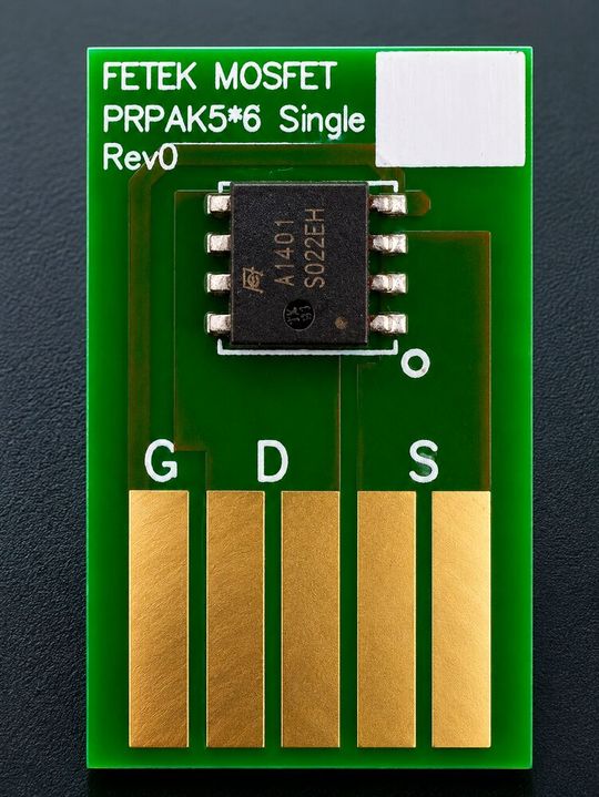
A Fetek MOSFET mounted on a test and evaluation board. Such setups allow the electrical and thermal behavior of a device to be examined under defined conditions.
(Bild: Fetek)
Fetek also names new-energy vehicles, robotics, industrial automation, energy infrastructure, aerospace, and conventional information and communications technology as markets that are expected to influence product development. Much of this is not exotic. These are mainly applications in which efficient power conversion is required in an increasing number of places.
Silicon is set to remain the core technology for now. According to Fetek, higher voltage classes as well as SiC and GaN are part of its mid- to long-term power device product strategy. Silicon power MOSFETs, however, remain the company’s established core platform for current customer applications.
A second source has to do more than look similar
For Europe, Fetek puts particular emphasis on its role as an alternative supplier. The company explicitly includes design-in support, technical cooperation and second-source flexibility in its positioning.
This is where a purchasing issue becomes a technical one again. Two MOSFETs with a similar voltage class and comparable RDS(on) do not necessarily behave in the same way. The more strongly an existing design has been optimized around one specific device, the more carefully an alternative has to be evaluated.
A true second source is therefore better qualified before a shortage occurs rather than during one. If a replacement is only tested once the original component is already unavailable, what looked like a simple component change can quickly become an engineering problem.
According to Fetek, the company wants to support customers in selecting technically suitable alternatives. For a supplier that is still far less familiar in Europe than the established MOSFET manufacturers, this is likely to be one of the key challenges. Cost competitiveness may attract initial interest, but device behavior, technical support and supply reliability are essential for a successful design-in.
Fabless means someone else has to manufacture
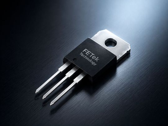
Silicon power MOSFET from Fetek. The company currently focuses its development mainly on low- and medium-voltage MOSFETs, aiming to balance conduction losses, switching behavior and thermal performance.
(Bild: Fetek)
Supply presents Fetek with an additional challenge. As a fabless company, it cannot support its claims of availability with its own wafer fab. Wafer production, assembly and test are organized together with manufacturing partners.
According to Fetek, capacity planning therefore starts at the wafer stage. Customer demand and forecasts are intended to feed into this planning, while production and delivery schedules are tracked through wafer manufacturing, assembly and test. Inventory and early communication with customers are meant to provide additional flexibility.
The written information is not enough to judge how well this model would perform during a major supply disruption. Another point is more relevant: a company that wants to act as a second source needs more than an electrically compatible device. It also needs to explain where that device will come from two or three years from now.
For European engineers considering Fetek as an additional source, that question may ultimately matter at least as much as another incremental improvement in RDS(on).
Building trust in the European market
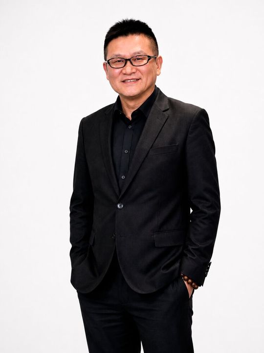
Simon Chang, Chairman and General Manager of Fetek. In the interview, he explains the company’s positioning in power semiconductors and second-source strategies.
(Bild: Fetek)
Fetek names industrial electronics, energy storage, motor drives, DC-DC conversion, power distribution and selected e-mobility applications as its main European target markets. Over the next three to five years, the company says it wants to work more closely with engineers, distributors and design-in partners, while increasing its visibility at events such as PCIM Europe and electronica.
That, however, is only the beginning of the more difficult part. A semiconductor supplier that is still relatively unknown has to persuade engineers to evaluate a new device, provide samples, answer technical questions and then remain a reliable supplier for years.
Perhaps that is why Fetek’s rather unspectacular message fits the company quite well. In its answers, it does not promise a MOSFET that beats every competitor on every specification. It promises an alternative in which technology, price, support and supply are intended to fit together. Fetek sees application-driven device selection, design-in cooperation and long-term supply planning as part of that approach.
Whether that works has to be proven in the individual design.
A second MOSFET on the bill of materials is not yet a true second source. It only becomes one when it can actually be used when it is needed. (sb)
Es ist für uns eine Selbstverständlichkeit, dass wir verantwortungsvoll mit Ihren personenbezogenen Daten umgehen. Sofern wir personenbezogene Daten von Ihnen erheben, verarbeiten wir diese unter Beachtung der geltenden Datenschutzvorschriften. Detaillierte Informationen finden Sie in unserer Datenschutzerklärung.
Einwilligung in die Verwendung von Daten zu Werbezwecken
Ich bin damit einverstanden, dass die Vogel Communications Group GmbH & Co. KG, Max-Planckstr. 7-9, 97082 Würzburg einschließlich aller mit ihr im Sinne der §§ 15 ff. AktG verbundenen Unternehmen (im weiteren: Vogel Communications Group) meine E-Mail-Adresse für die Zusendung von redaktionellen Newslettern nutzt. Auflistungen der jeweils zugehörigen Unternehmen können hier abgerufen werden.
Der Newsletterinhalt erstreckt sich dabei auf Produkte und Dienstleistungen aller zuvor genannten Unternehmen, darunter beispielsweise Fachzeitschriften und Fachbücher, Veranstaltungen und Messen sowie veranstaltungsbezogene Produkte und Dienstleistungen, Print- und Digital-Mediaangebote und Services wie weitere (redaktionelle) Newsletter, Gewinnspiele, Lead-Kampagnen, Marktforschung im Online- und Offline-Bereich, fachspezifische Webportale und E-Learning-Angebote. Wenn auch meine persönliche Telefonnummer erhoben wurde, darf diese für die Unterbreitung von Angeboten der vorgenannten Produkte und Dienstleistungen der vorgenannten Unternehmen und Marktforschung genutzt werden.
Meine Einwilligung umfasst zudem die Verarbeitung meiner E-Mail-Adresse und Telefonnummer für den Datenabgleich zu Marketingzwecken mit ausgewählten Werbepartnern wie z.B. LinkedIN, Google und Meta. Hierfür darf die Vogel Communications Group die genannten Daten gehasht an Werbepartner übermitteln, die diese Daten dann nutzen, um feststellen zu können, ob ich ebenfalls Mitglied auf den besagten Werbepartnerportalen bin. Die Vogel Communications Group nutzt diese Funktion zu Zwecken des Retargeting (Upselling, Crossselling und Kundenbindung), der Generierung von sog. Lookalike Audiences zur Neukundengewinnung und als Ausschlussgrundlage für laufende Werbekampagnen. Weitere Informationen kann ich dem Abschnitt „Datenabgleich zu Marketingzwecken“ in der Datenschutzerklärung entnehmen.
Falls ich im Internet auf Portalen der Vogel Communications Group einschließlich deren mit ihr im Sinne der §§ 15 ff. AktG verbundenen Unternehmen geschützte Inhalte abrufe, muss ich mich mit weiteren Daten für den Zugang zu diesen Inhalten registrieren. Im Gegenzug für diesen gebührenlosen Zugang zu redaktionellen Inhalten dürfen meine Daten im Sinne dieser Einwilligung für die hier genannten Zwecke verwendet werden. Dies gilt nicht für den Datenabgleich zu Marketingzwecken.
Recht auf Widerruf
Mir ist bewusst, dass ich diese Einwilligung jederzeit für die Zukunft widerrufen kann. Durch meinen Widerruf wird die Rechtmäßigkeit der aufgrund meiner Einwilligung bis zum Widerruf erfolgten Verarbeitung nicht berührt. Um meinen Widerruf zu erklären, kann ich als eine Möglichkeit das unter https://contact.vogel.de abrufbare Kontaktformular nutzen. Sofern ich einzelne von mir abonnierte Newsletter nicht mehr erhalten möchte, kann ich darüber hinaus auch den am Ende eines Newsletters eingebundenen Abmeldelink anklicken. Weitere Informationen zu meinem Widerrufsrecht und dessen Ausübung sowie zu den Folgen meines Widerrufs finde ich in der Datenschutzerklärung, Abschnitt Redaktionelle Newsletter.




:quality(80)/p7i.vogel.de/wcms/15/fd/15fdbabfc033d4c14b189fc5187feb52/0133536111v2.jpeg "Das europäische Forschungs- und Innovationsprojekt EuroQSS zielt darauf ab, einen offenen, interoperablen Quanten-Software-Stack zu entwickeln, der Hardware-Spezifikationen mit Abstraktion in Einklang bringt. Diese Infrastruktur soll hybride Arbeitsabläufe über verschiedene Quantencomputer und klassische Hochleistungs-Rechnersysteme hinweg unterstützen. (Bild: Fraunhofer IKS)")
:quality(80)/p7i.vogel.de/wcms/8a/9c/8a9caa85007d3299d7c3971d7eafc942/0133479121v2.jpeg "Leonard Neuberger und Linus Rüllmann von der Weißensee Kunsthochschule Berlin haben mit ihrem Any-Projekt den nationalen James Dyson Award 2026 erhalten. (Bild: Dyson)")
:quality(80)/p7i.vogel.de/wcms/71/a8/71a84cd5963e9ac263a77c788c339dc2/0133489329v3.jpeg "Eine Sandbox begrenzt die Handlungsmöglichkeiten eines KI-Agenten, ist aber keine undurchdringliche Barriere. Erst mehrere unabhängige Schutzebenen verhindern, dass ein Ausbruch unmittelbar den Zugriff auf produktive Systeme ermöglicht. (Bild: frei lizenziert)")
:quality(80)/p7i.vogel.de/wcms/b6/7d/b67d681fa57a0043e1a3d5f8527d1d08/0133522057v2.jpeg "TPVM ist eine eigenständige, zum Patent angemeldete Materialstruktur. Sie ist im Aluminiumguss oder im 3D-Druck realisierbar, industriell verfügbar und skalierbar. (Bild: Automoteam)")
:quality(80)/p7i.vogel.de/wcms/de/70/de70aa086973b1d297cb520d90bf19bb/0133423537v2.jpeg "Bluetooth Channel Sounding: Wie präzise die Messung ist, hängt jedoch auch von Antenne, HF-Design, Umgebung und Auswertealgorithmus ab. (Bild: KI-generiert)")
:quality(80)/p7i.vogel.de/wcms/f8/5c/f85c5fbc8487acc36917ad430a1135d5/0133483193v2.jpeg "Der Vitalsensor goVISCAN: Mittig sitzt die Multispektralkamera mit einem 3x3-Mikrolinsenarray, das die spektralen Bänder erfasst. Kreisförmig herum sind LEDs verbaut, die die Messszene beleuchten. (Bild: Fraunhofer IOF)")
:quality(80)/p7i.vogel.de/wcms/45/cb/45cbc6d920f7d6209bbe76229de0b589/0133555881v2.jpeg "Robotikmarkt Deutschland: Die Neuinstallationen von Industrierobotern sanken 2025 um acht Prozent auf rund 25.000 Einheiten. Besonders stark ging die Nachfrage in der Automobilindustrie zurück. (Bild: IFR)")
:quality(80)/p7i.vogel.de/wcms/58/93/5893d1c1946bcc25a9f8b8b939409aa2/0133444365v2.jpeg "KI trifft Lagerrobotik: Im Düsseldorfer Innovation Lab demonstriert Geekplus unter anderem humanoide Roboter, mobile Transportsysteme und das KI-Framework Gravity. (Bild: Geekplus)")
:quality(80)/p7i.vogel.de/wcms/00/97/0097c22b112065506b113f1ff07ea8ab/0133509585v2.jpeg "Ventuno Q RoadTest: soll der Element14-Community helfen, mittels Ventuno Q praktische Erkenntnisse aus realen Tests zu gewinnen. (Bild: Farnell/Element14)")
:quality(80)/p7i.vogel.de/wcms/52/90/52907b59eca824a3d40bd58c4577e910/0133428589v2.jpeg "(Bild: Raspberry PI)")
:quality(80)/p7i.vogel.de/wcms/bd/ba/bdba9a99b0b597968222d2758dd51812/0133237118v2.jpeg "Fetek bietet Leistungs-MOSFETs in unterschiedlichen Gehäusebauformen an. Für eine geeignete Second Source reicht die mechanische und elektrische Ähnlichkeit allein allerdings nicht aus – entscheidend ist das Verhalten im konkreten Design. (Bild: Fetek)")
:quality(80)/p7i.vogel.de/wcms/da/2d/da2d155884f924e1d6ea84b77cf48d5c/0133352781v2.jpeg "Die SMD-Sicherungen der 48MH-Serie von Conquer sind für hohe Ströme ausgelegt und für den Einsatz in KI-Servern und Rechenzentren vorgesehen. Die kompakte Bauform ermöglicht eine automatisierte Bestückung. (Bild: Conquer)")
:quality(80)/p7i.vogel.de/wcms/5f/77/5f778eafd9e4415cd00274ad9a58e42a/0133462125v2.jpeg "Wandler: Integrierte GaN-Buck- und Boost-Wandler für den Mittelspannungsbereich benötigen 50 % weniger Platz als Alternativen auf Siliziumbasis, ohne dass dabei Einbußen beim Wirkungsgrad entstehen. (Bild: TI)")
:quality(80)/p7i.vogel.de/wcms/3d/67/3d6777d7a99bdf88f86798cd73451538/0133004756v2.jpeg "Die AGI-CPU von Arm wurde im März 2026 angekündigt. Im Rahmen der Hot Chips 2026 sind die Entwickler ins Detail gegangen. (Bild: Arm)")
:quality(80)/p7i.vogel.de/wcms/8a/2e/8a2e7d2a89ffe55c545dd6c831ed154e/0132246788v2.jpeg "Über 500 Teilnehmer, 120 Referenten: Die FPGA Conference Europe platzte in diesem Jahr aus allen Nähten – und wurde ihrem Anspruch als Leitkongress der FPGA-Welt einmal mehr gerecht. (Bild: Tobi Giessen)")
:quality(80)/p7i.vogel.de/wcms/06/a1/06a158e32b18d99fcea65547cec5d4c7/0132069489v2.jpeg "Mit direkter Integration von Speicher ins Chip-Package verspricht AMD mit dem Versal Premium Gen 2 SoC eine schnellere Datenübertragung, verringerte Latenz und einem potentiell geringere Stromverbrauch. (Bild: AMD)")
:quality(80)/p7i.vogel.de/wcms/86/2a/862afb1de8423bb7401098a2fd268281/0131792672v2.jpeg "Bild 1: Ein Spannungsversorgungskonzept für Lasten, welche eine vorgegebene Ein- und Abschaltreihenfolge (Sequencing) benötigen. (Bild: ADI)")
:quality(80)/p7i.vogel.de/wcms/60/e7/60e71d2e90f60e5ddef056cb234724e0/0133466221v2.jpeg "Strom unter Last: Das Stromdichteprofil zeigt die Verteilung im Hochleistungs-IGBT-Modul. (Bild: Comsol)")
:quality(80)/p7i.vogel.de/wcms/31/20/3120ef4dfc9af325be75131132df2e6a/0133343322v2.jpeg "Aerodynamik-Weltrekord – Mission Efficiency setzt mit einem cW-Wert von 0,158 die neue Bestmarke aller straßenzugelassenen Autos. (Bild: Volkswagen AG)")
:quality(80)/p7i.vogel.de/wcms/a9/3c/a93cb3af2dd2d3d5a43365ea69a3d8a1/0133339957v2.jpeg "Der am MIT entwickelte Algorithmus „Hard Flow“ verspricht, vortrainierten generativen KI-Modellen dabei zu helfen, strenge Einschränkungen einzuhalten und gleichzeitig die Lösungsqualität zu verbessern, ohne dass ein erneutes Training erforderlich ist. (Bild: Dall-E / KI-generiert)")
:quality(80)/p7i.vogel.de/wcms/06/f8/06f81a56e8b4dba56769b65bea11196c/0133538220v2.jpeg "Aufbau zur Messung der Wärmeleitfähigkeit bei kryogenen Temperaturen. Das Kryo-Labor ergänzt die Infrastruktur für Quantencomputing-Komponenten. (Bild: TU Chemnitz)")
:quality(80)/p7i.vogel.de/wcms/1d/31/1d311b67f71d045fb28883d6b8ce6469/0133505895v2.jpeg "Das Testsystem „Iris 100“ für die hochpräzise Volumenfertigung von microLEDs nutzt ein Spektrometer und eine hochauflösende Kamera. (Bild: Teradyne)")
:quality(80)/p7i.vogel.de/wcms/6b/0c/6b0cd14955e1df9cddc90de9a6209ea6/0133376931v2.jpeg "Parallele Testabläufe: Mit dem von MCD entwickelten Software TestMate lassen sich mehrere Testsequenzen innerhalb einer Instanz parallel und asynchron ausführen. (Bild: MCD Elektronik)")
:quality(80)/p7i.vogel.de/wcms/69/20/6920b333a42be206f380befd3ae34c36/0133394583v2.jpeg "Die beiden Cäsium-Fontänenuhren der PTB liefern die gesetzliche Zeit für die gesamte Bundesrepublik. Die verwendeten Laser werden jetzt digital von einer AWG-Messkarte gesteuert. (Bild: PTB)")
:quality(80)/p7i.vogel.de/wcms/bb/d2/bbd2a0fef7f8b760b98f16c8a8b51376/0133546934v2.jpeg "EEBUS-Zertifizierung: Die Energy-Manager-Plattform von TQ ermöglicht den standardisierten Datenaustausch zwischen Energiemanagementsystemen und angeschlossenen Anlagen, um Stromverbrauch und Einspeisung bedarfsgerecht zu steuern. (Bild: TQ)")
:quality(80)/p7i.vogel.de/wcms/47/0e/470e414076f52c39059cede15c1ea71e/0133496024v2.jpeg "Intelligente Fertigung: Daten, KI und Robotik wachsen in der SMT-Fertigung zunehmend zusammen. Vernetzte Systeme erkennen Prozessabweichungen, steuern Materialflüsse und leiten immer häufiger selbstständig Maßnahmen ein. (Bild: ASMPT SMT Solutions)")
:quality(80)/p7i.vogel.de/wcms/d4/2d/d42d81c60f05b8a27af2babe858b1c40/0133430053v2.jpeg "Bauteilkennzeichnung: Der laserbeschriftete Sensor kombiniert Data-Matrix-Code und Klarschrift für eine dauerhaft maschinen- und menschenlesbare Kennzeichnung. (Bild: FOBA Laser Marking + Engraving)")
:quality(80)/p7i.vogel.de/wcms/04/b9/04b948db62de8d70b7424a2607cb74de/0133453624v2.jpeg "Waferfertigung bei TSMC. Die Chipfertigung in den USA droht, trotz massivem Ausbau an Fertigungsstätten in einen Flaschenhals zu geraten. Nur etwa drei Prozent aller Studenten aus geigneten Fachbereichen haben laut einer Studie von McKinsey und dem Halbleiterverband SEMI vor, in die Hardware-Entwicklung zu gehen, und ziehen Bereiche wie KI oder Software Engineering vor. (Bild: TSMC)")
:quality(80)/p7i.vogel.de/wcms/66/25/66252e7176c957416bf64e8c693128bf/0133550680v2.jpeg "Nexperia und Tata Electronics schließen strategische Partnerschaft entlang der Halbleiter-Wertschöpfungskette. (Bild: Tata)")
:quality(80)/p7i.vogel.de/wcms/d1/8a/d18a13c7f00027ced756217817f29be7/0133550198v2.jpeg "Vom Wafer zur Anwendung: Der Chips Act 2.0 soll künftig nicht nur Fertigungskapazitäten fördern, sondern auch die Nachfrage nach Halbleitern aus Europa stärker in den Blick nehmen. (Bild: Dall-E / KI-generiert)")
:quality(80)/p7i.vogel.de/wcms/6b/1d/6b1dde86fdb120b4cf9b8bc8573c415a/0133056789v3.jpeg "Wir bezahlen für Systeme, die menschliche Arbeit übernehmen, ohne bislang geklärt zu haben, wie die dadurch entstehende Wertschöpfung künftig verteilt werden soll. (Bild: frei lizenziert)")
:quality(80)/p7i.vogel.de/wcms/47/20/47201c1ce3692dbdb4e7e62709de4e16/0132649717v3.jpeg "Ingenieurberufe verändern sich: Neben der aktuellen Konjunktur treiben Digitalisierung, KI und neue Technologien den Bedarf an kontinuierlicher Qualifizierung. (Bild: frei lizenziert)")
:quality(80)/p7i.vogel.de/wcms/4e/41/4e4159d1e93e67d47bd2f51a90691b23/0131548978v2.jpeg "Transformation im Engineering: KI-gestützte Systeme generieren zunehmend selbstständig Schaltschranklayouts und entlasten Konstrukteure von zeitraubenden Routineaufgaben. (Bild: WSCAD)")
:quality(80)/p7i.vogel.de/wcms/2f/0c/2f0cdaf3c1041b3592bd71e44edd4aea/0133352797v2.jpeg "Conquer’s 48MH series SMD fuses are designed for high-current applications in AI servers and data centers. Their compact form factor supports automated assembly. (Bild: Conquer)")
:quality(80)/p7i.vogel.de/wcms/3e/52/3e52caf04ffc0446ac34990ea5fa95b6/0133240185v2.jpeg "Surge-fester MELF-Widerstand aus der SRM-Serie von Firstohm. Die Baureihe ist für Anwendungen ausgelegt, in denen kurzzeitig hohe Energien und wiederholte Entladeimpulse auftreten können. (Bild: Firstohm)")