A fast GaN HEMT alone is not enough. At 650 V, package and PCB parasitics and thermal paths determine switching performance, losses, and susceptibility to ringing, EMI, false turn-on, and overheating.
Packaging: Control parasitics, stabilize switching, and get heat out of high-density converters.
(Source: ROHM Semiconductor)
Gallium nitride (GaN) high electron mobility transistors (HEMT) switch current and voltage faster than any other kind of power device now in the market. That speed enables compact, efficient power conversion, but it also magnifies effects that were easier to ignore when using slower power devices. Tens of nanohenries in a commutation path, for example, can generate meaningful voltage error when current changes rapidly. The underlying relationship is straightforward: The voltage across an inductor is equal to the inductance multiplied by the rate of change of the current.
As di/dt rises, the voltage produced across even a small inductance rises with it. In hardware, the result may appear as drain overshoot, oscillation, gate bounce, elevated EMI, or unwanted switching. Circuit simulations do not always reveal these behaviours, especially when nonlinear device characteristics and extracted package or layout parasitics are not modeled.
The challenge extends beyond the package of the power device. PCB geometry, grounding, probing, copper distribution, and test connections can all alter measured waveforms. Certain parasitic parameters also vary with operating conditions such as drain-source voltage, making physical measurement and model correlation more difficult.
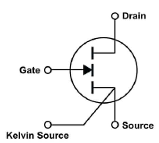
Figure 1. Power transistor with a dedicated Kelvin-source connection.
(Source: ROHM Semiconductor)
Why the Move to 650 V Raises the Stakes for GaN Packaging and PCB Design
Moving from lower-voltage power stages into the 650 V range is not simply a matter of scaling an existing gate-drive and layout concept. As the DC bus approaches the device rating, there is less tolerance for turn-off overshoot. At the same time, faster edge rates increase the voltage induced across the DC-link and commutation-loop inductances.
Several mechanisms then interact:
Commutation-loop inductance resonates with circuit capacitance, producing ringing and potentially destructive drain-source voltage peaks.
Common-source inductance shifts the apparent source potential and therefore distorts the gate-source voltage seen by the device.
Gate-loop inductance changes the impedance presented to the driver and reshapes the gate-current waveform.
High dv/dt forces displacement current through the Miller capacitance. If the off-state gate path is too weak, the complementary switch can briefly cross its turn-on voltage threshold.
That final mechanism can trigger false turn-on in a half bridge. If the high-side and low-side devices conduct together, the bridge creates a low-impedance path from the supply to ground. The resulting shoot-through current can damage both switches. Package choices that reduce inductance and improve the gate signal speed and quality contribute directly to switching robustness.
A Separate Gate Reference: the Kelvin-Source
Kelvin terminal sensing is a concept from precision measurement, where separate force and sense conductors prevent lead resistance from disturbing a voltage measurement. Power packages apply a related idea to gate control: a dedicated Kelvin-source terminal returns the gate-drive current independently of the high-current source path.
Separating these paths prevents the voltage developed across the power-source inductance from entering the gate loop. The driver receives a cleaner source reference, as common-source feedback is minimized, and the gate signal is less likely influenced by the load current. Decoupling of gate and power loops via Kelvin terminals can lower the switching loss and reduce oscillation.
Electrical Design and Thermal Design Are the Same Packaging Problem
Low inductance alone is not enough. The package must also conduct heat from the chip into the board, heat sink, and surrounding air. Designers initially use two thermal parameters when comparing options:
θJC: junction-to-case thermal resistance, sometimes specified separately for the top and bottom heat-flow paths.
θJA: junction-to-ambient thermal resistance, relevant to the complete path into the surrounding air and normally evaluated without an external heat sink.
Electrical and thermal improvements can be achieved simultaneously. Flip-chip construction can shorten interconnects while improving the path from the chip to the external terminals. Broad lead frames and larger solder interfaces can simultaneously reduce impedance, spread current, and conduct heat. On the boundary of the package exterior, PCB copper, thermal vias, airflow, and a directly attached heat sink can extend the cooling path.
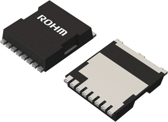
Figure 2. Rohm GNP30xxTD-Z in the TOLL-8N package.
(Source: ROHM Semiconductor)
How the TOLL Package Addresses Both Constraints
Rohm Semiconductor provides its third-generation, 650 V enhancement-mode GaN HEMT discrete products, GNP30xxYY-Z in the surface-mount TOLL-8N package. For example, the GNP3050TD-Z combines 50 mΩ on-resistance with 4.3 nC gate charge in a roughly 12 mm × 10 mm × 2.4 mm body, targeting high-frequency converters where board area and power density are critical. The package replaces long through-hole leads with short conductors. There are eight terminals on one side: one gate pin, one Kelvin-source pin, and six power-source contacts, originating from the thermal pad. Sharing current across six source contacts lowers current density and parasitic impedance while increasing the available thermal interface. A wide drain contact on the opposite side provides a similarly broad electrical and heat-flow path.
Stand: 08.12.2025
Es ist für uns eine Selbstverständlichkeit, dass wir verantwortungsvoll mit Ihren personenbezogenen Daten umgehen. Sofern wir personenbezogene Daten von Ihnen erheben, verarbeiten wir diese unter Beachtung der geltenden Datenschutzvorschriften. Detaillierte Informationen finden Sie in unserer Datenschutzerklärung.
Einwilligung in die Verwendung von Daten zu Werbezwecken
Ich bin damit einverstanden, dass die Vogel Communications Group GmbH & Co. KG, Max-Planckstr. 7-9, 97082 Würzburg einschließlich aller mit ihr im Sinne der §§ 15 ff. AktG verbundenen Unternehmen (im weiteren: Vogel Communications Group) meine E-Mail-Adresse für die Zusendung von redaktionellen Newslettern nutzt. Auflistungen der jeweils zugehörigen Unternehmen können hier abgerufen werden.
Der Newsletterinhalt erstreckt sich dabei auf Produkte und Dienstleistungen aller zuvor genannten Unternehmen, darunter beispielsweise Fachzeitschriften und Fachbücher, Veranstaltungen und Messen sowie veranstaltungsbezogene Produkte und Dienstleistungen, Print- und Digital-Mediaangebote und Services wie weitere (redaktionelle) Newsletter, Gewinnspiele, Lead-Kampagnen, Marktforschung im Online- und Offline-Bereich, fachspezifische Webportale und E-Learning-Angebote. Wenn auch meine persönliche Telefonnummer erhoben wurde, darf diese für die Unterbreitung von Angeboten der vorgenannten Produkte und Dienstleistungen der vorgenannten Unternehmen und Marktforschung genutzt werden.
Meine Einwilligung umfasst zudem die Verarbeitung meiner E-Mail-Adresse und Telefonnummer für den Datenabgleich zu Marketingzwecken mit ausgewählten Werbepartnern wie z.B. LinkedIN, Google und Meta. Hierfür darf die Vogel Communications Group die genannten Daten gehasht an Werbepartner übermitteln, die diese Daten dann nutzen, um feststellen zu können, ob ich ebenfalls Mitglied auf den besagten Werbepartnerportalen bin. Die Vogel Communications Group nutzt diese Funktion zu Zwecken des Retargeting (Upselling, Crossselling und Kundenbindung), der Generierung von sog. Lookalike Audiences zur Neukundengewinnung und als Ausschlussgrundlage für laufende Werbekampagnen. Weitere Informationen kann ich dem Abschnitt „Datenabgleich zu Marketingzwecken“ in der Datenschutzerklärung entnehmen.
Falls ich im Internet auf Portalen der Vogel Communications Group einschließlich deren mit ihr im Sinne der §§ 15 ff. AktG verbundenen Unternehmen geschützte Inhalte abrufe, muss ich mich mit weiteren Daten für den Zugang zu diesen Inhalten registrieren. Im Gegenzug für diesen gebührenlosen Zugang zu redaktionellen Inhalten dürfen meine Daten im Sinne dieser Einwilligung für die hier genannten Zwecke verwendet werden. Dies gilt nicht für den Datenabgleich zu Marketingzwecken.
Recht auf Widerruf
Mir ist bewusst, dass ich diese Einwilligung jederzeit für die Zukunft widerrufen kann. Durch meinen Widerruf wird die Rechtmäßigkeit der aufgrund meiner Einwilligung bis zum Widerruf erfolgten Verarbeitung nicht berührt. Um meinen Widerruf zu erklären, kann ich als eine Möglichkeit das unter https://contact.vogel.de abrufbare Kontaktformular nutzen. Sofern ich einzelne von mir abonnierte Newsletter nicht mehr erhalten möchte, kann ich darüber hinaus auch den am Ende eines Newsletters eingebundenen Abmeldelink anklicken. Weitere Informationen zu meinem Widerrufsrecht und dessen Ausübung sowie zu den Folgen meines Widerrufs finde ich in der Datenschutzerklärung, Abschnitt Redaktionelle Newsletter.
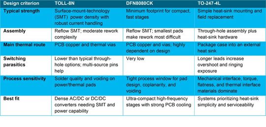
Table 1. Relative package comparison for common power-stage design priorities.
(Source: ROHM Semiconductor)
Selecting the Right GaN Package for the System’s Requirements
Selecting a package for an application depends on how the design must balance switching speed, footprint, heat removal, assembly, and serviceability. GaN HEMT power devices are available in TOLL and DFN8080 packages. In general, even for wide-bandgap transistors, the TO-247-4L package is still an expected commodity.
Conclusion: Package Architecture Unlocks the Device
The performance advantage of 650 V GaN can only be realized when the surrounding interconnect and thermal structure are designed for the same speed and power density as the semiconductor itself. At fast current and voltage transitions, package inductance can no longer be treated as a minor detail, and the package must also provide an efficient route for heat to leave the chip.
TOLL-8N addresses these requirements through short conductors, separated source terminals including a dedicated Kelvin-source connection, and broad electrical and thermal interfaces. These features reduce the package-related effects that contribute to overshoot, gate disturbance, switching loss, and thermal limitation. For the GNP30xxYY-Z product line from Rohm, the package is therefore not merely a housing: it is a central part of how the 650 V GaN HEMT delivers high-frequency, high-density converter performance. (mr)