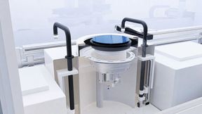
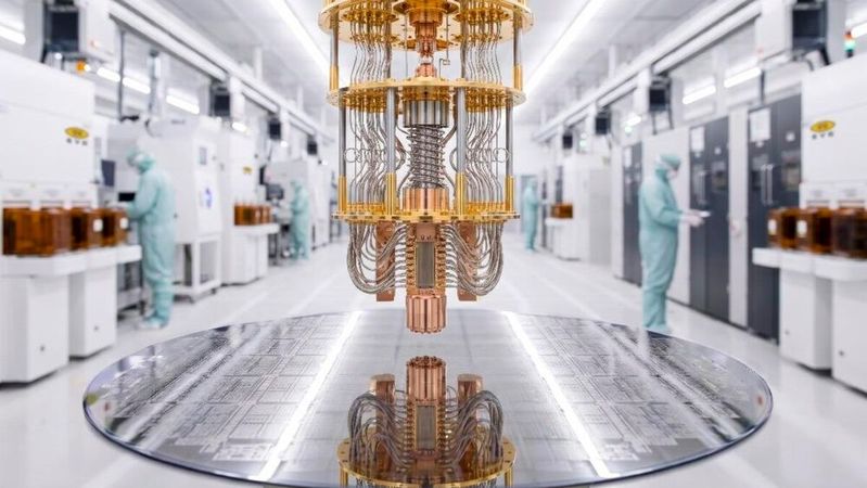
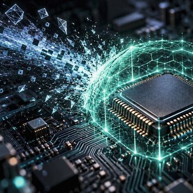
EV Group applies its expertise in wafer bonding, heterogeneous integration and lithography to support the development and manufacturing of next-generation quantum chips.
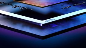
Quantum Chip Manufacturing: Advanced wafer bonding and heterogeneous integration are key to scaling quantum computing.
(Source: EVG)
As quantum computing moves from laboratory demonstrations towards increasingly powerful systems, the semiconductor industry faces a growing manufacturing challenge: how to scale the number of qubits while maintaining the performance and reliability required for fault-tolerant operation. Advanced packaging and heterogeneous integration technologies are emerging as important enablers in addressing this challenge. Austrian semiconductor equipment supplier EV Group (EVG) is leveraging its established process expertise to support quantum chip developers in tackling these requirements.
The company is applying its capabilities in wafer bonding, lithography, thin-wafer processing and photonics manufacturing to help customers develop and validate new quantum device architectures and associated manufacturing processes. EVG will present its technology portfolio for quantum computing and other advanced applications at SEMICON Europa.
Manufacturing complexity increases
According to McKinsey & Company, quantum computing could generate up to US$2.7 trillion in economic value worldwide by 2035. However, translating the technology's potential into practical applications requires overcoming considerable technical and manufacturing hurdles.
One of the most significant challenges is increasing the number of qubits – the fundamental units of quantum information – without compromising device performance. Since qubits are highly susceptible to environmental disturbances and operational errors, fault-tolerant quantum computing requires large numbers of physical qubits to implement effective quantum error correction.
The manufacturing implications are substantial. Different quantum computing architectures rely on different materials, device structures and operating principles. Integrating these components requires highly precise processes, including high-density interconnections, the integration of dissimilar materials and increasingly complex three-dimensional chip architectures.
Advanced packaging technologies can provide important building blocks for this next stage of development. By enabling the integration of different materials and functional components, they can help address the requirements of increasingly sophisticated quantum processors while preserving the characteristics essential to their operation.
Different quantum architectures
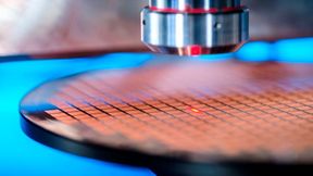
EVG's technology portfolio includes fusion and hybrid bonding, high-vacuum oxide-free bonding, digital and nanoimprint lithography, as well as temporary bonding and debonding for thin-wafer processing. These processes address critical requirements for wafer alignment, material integration, interconnection and patterning across a range of quantum computing approaches.
The company's Heterogeneous Integration Competence Center (HICC) and NILPhotonics Competence Center provide additional infrastructure and process expertise. Together, these facilities enable customers to investigate materials, develop process flows and validate new device concepts under semiconductor manufacturing conditions.
The relevance of these technologies varies depending on the quantum computing architecture. In superconducting quantum devices, for example, oxide-free bonding processes can support the formation of superconducting interconnects and three-dimensional device integration.
For photonic quantum computing, fusion and oxide-free bonding can enable the integration of III-V semiconductor materials and materials with high Pockels coefficients onto optical waveguides. Such integration is important for developing advanced photonic functionality. In emerging spin-qubit architectures, hybrid bonding offers a route towards ultra-high-density interconnections.
Trapped-ion quantum computing presents another set of integration challenges. Here, EVG has worked with research partners to develop low-temperature metal bonding processes that allow ion-trap and photonic chiplets fabricated on different substrate materials to be integrated.
Stand: 08.12.2025
Es ist für uns eine Selbstverständlichkeit, dass wir verantwortungsvoll mit Ihren personenbezogenen Daten umgehen. Sofern wir personenbezogene Daten von Ihnen erheben, verarbeiten wir diese unter Beachtung der geltenden Datenschutzvorschriften. Detaillierte Informationen finden Sie in unserer Datenschutzerklärung.
Einwilligung in die Verwendung von Daten zu Werbezwecken
Ich bin damit einverstanden, dass die Vogel Communications Group GmbH & Co. KG, Max-Planckstr. 7-9, 97082 Würzburg einschließlich aller mit ihr im Sinne der §§ 15 ff. AktG verbundenen Unternehmen (im weiteren: Vogel Communications Group) meine E-Mail-Adresse für die Zusendung von redaktionellen Newslettern nutzt. Auflistungen der jeweils zugehörigen Unternehmen können hier abgerufen werden.
Der Newsletterinhalt erstreckt sich dabei auf Produkte und Dienstleistungen aller zuvor genannten Unternehmen, darunter beispielsweise Fachzeitschriften und Fachbücher, Veranstaltungen und Messen sowie veranstaltungsbezogene Produkte und Dienstleistungen, Print- und Digital-Mediaangebote und Services wie weitere (redaktionelle) Newsletter, Gewinnspiele, Lead-Kampagnen, Marktforschung im Online- und Offline-Bereich, fachspezifische Webportale und E-Learning-Angebote. Wenn auch meine persönliche Telefonnummer erhoben wurde, darf diese für die Unterbreitung von Angeboten der vorgenannten Produkte und Dienstleistungen der vorgenannten Unternehmen und Marktforschung genutzt werden.
Meine Einwilligung umfasst zudem die Verarbeitung meiner E-Mail-Adresse und Telefonnummer für den Datenabgleich zu Marketingzwecken mit ausgewählten Werbepartnern wie z.B. LinkedIN, Google und Meta. Hierfür darf die Vogel Communications Group die genannten Daten gehasht an Werbepartner übermitteln, die diese Daten dann nutzen, um feststellen zu können, ob ich ebenfalls Mitglied auf den besagten Werbepartnerportalen bin. Die Vogel Communications Group nutzt diese Funktion zu Zwecken des Retargeting (Upselling, Crossselling und Kundenbindung), der Generierung von sog. Lookalike Audiences zur Neukundengewinnung und als Ausschlussgrundlage für laufende Werbekampagnen. Weitere Informationen kann ich dem Abschnitt „Datenabgleich zu Marketingzwecken“ in der Datenschutzerklärung entnehmen.
Falls ich im Internet auf Portalen der Vogel Communications Group einschließlich deren mit ihr im Sinne der §§ 15 ff. AktG verbundenen Unternehmen geschützte Inhalte abrufe, muss ich mich mit weiteren Daten für den Zugang zu diesen Inhalten registrieren. Im Gegenzug für diesen gebührenlosen Zugang zu redaktionellen Inhalten dürfen meine Daten im Sinne dieser Einwilligung für die hier genannten Zwecke verwendet werden. Dies gilt nicht für den Datenabgleich zu Marketingzwecken.
Recht auf Widerruf
Mir ist bewusst, dass ich diese Einwilligung jederzeit für die Zukunft widerrufen kann. Durch meinen Widerruf wird die Rechtmäßigkeit der aufgrund meiner Einwilligung bis zum Widerruf erfolgten Verarbeitung nicht berührt. Um meinen Widerruf zu erklären, kann ich als eine Möglichkeit das unter https://contact.vogel.de abrufbare Kontaktformular nutzen. Sofern ich einzelne von mir abonnierte Newsletter nicht mehr erhalten möchte, kann ich darüber hinaus auch den am Ende eines Newsletters eingebundenen Abmeldelink anklicken. Weitere Informationen zu meinem Widerrufsrecht und dessen Ausübung sowie zu den Folgen meines Widerrufs finde ich in der Datenschutzerklärung, Abschnitt Redaktionelle Newsletter.
Beyond these bonding technologies, nanoimprint and digital lithography can support the fabrication of specialized optical structures, while temporary bonding and debonding processes provide additional options for advanced packaging and thin-wafer handling.
The Importance of Collaboration
EVG's activities in quantum computing extend beyond the provision of process equipment. The company is also involved in collaborative research and development initiatives aimed at addressing the manufacturing requirements of emerging quantum technologies.
One example is its strategic partnership with Silicon Austria Labs in the CHAMP-ION pilot line project. The initiative is developing Europe's first open-access pilot line for the industrial-scale production of ion-trap quantum chips. The project is intended to help bridge the gap between research-oriented device development and scalable manufacturing.
EVG has also recently announced a collaboration with Xanadu, a developer of photonic quantum computing technology. Together with its participation in other research activities, this engagement reflects the growing importance of semiconductor manufacturing expertise in the development of quantum hardware.
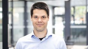
„Quantum computing is not a single technology, but a collection of fundamentally different approaches, each with its own materials and manufacturing requirements,” said Dr. Bernd Dielacher, Director of Business Development at EVG. „As developers work to scale these technologies, the challenge is not simply increasing the number of qubits but finding ways to integrate them in increasingly complex chip architectures without compromising performance.“
He added that EVG's process portfolio, combined with its experience in advanced packaging and heterogeneous integration, can help customers develop practical manufacturing solutions for a new generation of quantum devices.
As quantum computing architectures continue to evolve, the ability to integrate different materials, functional components and device structures with semiconductor-level precision is likely to become increasingly important. While the requirements differ considerably between quantum technologies, advances in wafer bonding, lithography and heterogeneous integration are positioning established semiconductor manufacturing processes as key contributors to the industrialization of quantum hardware. (sb)