Super-junction MOSFETs Influence of parasitic components in switching behavior
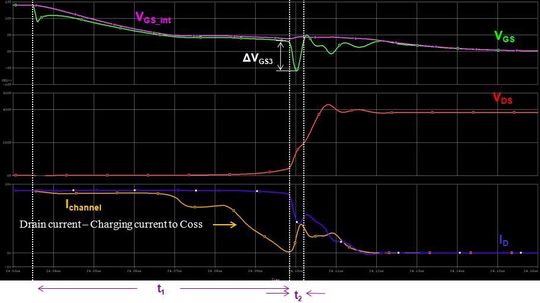
The faster switching of the power MOSFETs enable higher power conversion efficiency. However, parasitic components in the devices and boards are involving switching characteristics more as the switching speed is getting faster. This creates unwanted side effects, like high voltage or current spikes or poor EMI performance.
Anbieter zum Thema

Power MOSFET technology has been developed towards higher cell density for lower on-resistance. There are, however, silicon limits for significant reduction in the on-resistance with the conventional planar MOSFET technology because of its exponential increase in on-resistance according to the increase of blocking capability. One of efforts to overcome the silicon limit is super-junction technology in high-voltage power MOSFETs.
The super-junction technology can dramatically reduce both on-resistance and parasitic capacitances, which usually are in trade-off. With smaller parasitic capacitances, the super-junction MOSFETs have extremely fast switching characteristics and reduced switching losses. However, fast transitions in voltage and current result in high-frequency noises and radiated EMI.
To achieve low noise radiation, high values of parasitic capacitances are required. There is direct conflict in parasitic capacitance requirements. Based on recent system trends, improving efficiency is a critical goal and going with slow switching device just for EMI is not an optimized solution. In part 1, we will discuss about influence of parasitic components to achieve balance between these considerations when designing with super-junction MOSFETs.
Influence of Circuit Parameters on Switching Characteristics
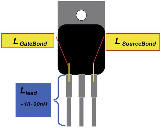
Package & Layout Parasitics: To drive fast-switching super-junction MOSFETs, it is also necessary to understand the influence of the prasitics in package and PCB layout on switching performance. The super-junction MOSFETs are mainly used in the voltage range of 500-600 V. In these voltage ratings, the most popular packages are industry standard TO-220, TO-247, TO-3P, and TO-263. The impact of the package on performance is limited due to the fact that the internal gate and source bonding wire length are fixed.
Only the length of the lead can be changed to reduce the source inductance of the package. Typical lead inductance of 10 nH, as shown in Figure 1(a), doesn’t look like much, but a turn-off a current with di/dt=500 A / µs is easily possible with these MOSFETs. The voltage across this inductance is VIND = 5 V and, with a turn-off di/dt of 1,000 A / µs, the induced voltage is VIND = 10 V.
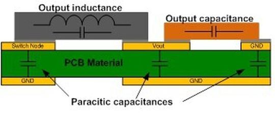
This short calculation shows that the complete source inductance, not only the lead inductance of the package, must be reduced to acceptable value. Another source of noise is layout parasitic. Two types are visible: parasitic inductance and parasitic capacitance. 1 cm of trace pitch has an inductance of 6-10 nH, which can be reduced by adding one layer on the topside of the PCB and a GND plane on the bottom side of the PCB.


The other type is the parasitic capacitances. Figure 1(b) shows the principles of capacitive layout parasitics. The capacitance between one trace is immediately over the other trace or GND plane on the other side of the PCB. The second one is the capacitance built up between the device and the GND plane. Two parallel traces on both sides of PCB increase capacitance, but also reduce the inductance of the loop, resulting in less magnetic noise radiation.
(ID:42669669)


:quality(80)/p7i.vogel.de/wcms/46/7c/467c0afffbfd10c3553c2888a4a6289f/0130479810v3.jpeg)
:quality(80)/p7i.vogel.de/wcms/12/3d/123d9eb2c2e4ce13296371a2ad3718a4/0130412664v2.jpeg)
:quality(80)/p7i.vogel.de/wcms/d8/78/d878b7bfc23826e6ddfce42443836d28/0130384280v2.jpeg)
:quality(80)/p7i.vogel.de/wcms/13/20/13208d1c2797edd67d9ff216b403726b/0130471595v3.jpeg)
:quality(80)/p7i.vogel.de/wcms/38/cb/38cbe19e814dd30b94780bc3946547ab/0130446533v2.jpeg)
:quality(80)/p7i.vogel.de/wcms/a3/3e/a33e6d8a927d539ec6c3a0537f48f0f1/0130440028v2.jpeg)
:quality(80)/p7i.vogel.de/wcms/6b/61/6b61373f1c3f06f7f9343e6b0f0e9cc8/0130225062v1.jpeg)
:quality(80)/p7i.vogel.de/wcms/15/93/1593dd152e6d58c5fc5da0d331777c54/0130357398v2.jpeg)
:quality(80)/p7i.vogel.de/wcms/c2/88/c28805ea7b2261235475146a5b0c61f8/0130313028v2.jpeg)
:quality(80)/p7i.vogel.de/wcms/fa/8d/fa8dedee195f29c33c89d86311c258ee/0130104146v2.jpeg)
:quality(80)/p7i.vogel.de/wcms/cc/13/cc1378375499a26b5ddbb309d2155acb/0130085649v2.jpeg)
:quality(80)/p7i.vogel.de/wcms/6d/91/6d91abfa1b16ffcf470c7147facd7aa8/0130387695v2.jpeg)
:quality(80)/p7i.vogel.de/wcms/85/b0/85b0b32128f6d1968e975043f1e0b67b/0130342166v3.jpeg)
:quality(80)/p7i.vogel.de/wcms/1a/53/1a539631c940d184689460600bd2b395/0130410666v2.jpeg)
:quality(80)/p7i.vogel.de/wcms/10/45/1045969e69a1db4aaa73d0f74f55cc02/0129962687v2.jpeg)
:quality(80)/p7i.vogel.de/wcms/cd/32/cd3243e4a9a6476265ef6ea9463dfbd8/0129852659v2.jpeg)
:quality(80)/p7i.vogel.de/wcms/c7/f6/c7f61d0437c7f8fca3c6ff947ba2ad62/0129322490v2.jpeg)
:quality(80)/p7i.vogel.de/wcms/ba/e4/bae4e54395e5a53088060531ef99b814/0130359274v2.jpeg)
:quality(80)/p7i.vogel.de/wcms/35/af/35af7dd326d198475d06fbb69aa600b5/0130175971v2.jpeg)
:quality(80)/p7i.vogel.de/wcms/c0/2e/c02e7bf72bfc434888c37100e2511681/0130127767v3.jpeg)
:quality(80)/p7i.vogel.de/wcms/7c/04/7c04916c305164fb10bc6cb05b51d934/0130431065v2.jpeg)
:quality(80)/p7i.vogel.de/wcms/64/e5/64e5e333492f182ab7df5ab4c2b54c1e/0130463252v2.jpeg)
:quality(80)/p7i.vogel.de/wcms/0a/95/0a95db4508128c4e11d5d268bf2c0a77/0130440053v2.jpeg)
:quality(80)/p7i.vogel.de/wcms/b3/65/b365dd5433c8b6d36c56c92b72f5b368/0130401081v2.jpeg)
:quality(80)/p7i.vogel.de/wcms/85/c0/85c0cdd8fd326013aed52ca96777c998/0130426877v2.jpeg)
:quality(80)/p7i.vogel.de/wcms/f0/78/f07826d6c4e995980f1ada3377416aac/0130403626v4.jpeg)
:quality(80)/p7i.vogel.de/wcms/b6/c8/b6c8f7732da417bda3d298412f4c0ed8/0130453104v2.jpeg)
:quality(80)/p7i.vogel.de/wcms/47/ce/47ce64bad7990f276f68cbb24505f6dd/0130472850v2.jpeg)
:quality(80)/p7i.vogel.de/wcms/15/56/15564dea31861c376a385658c3b961a3/0130465243v2.jpeg)
:quality(80)/p7i.vogel.de/wcms/98/ad/98ad595a6372aae8dbeac71681d23f41/0130450258v2.jpeg)
:quality(80)/p7i.vogel.de/wcms/bf/2a/bf2aad428ab1a80e6738fdbdc2efeb7e/0130453420v2.jpeg)
:quality(80)/p7i.vogel.de/wcms/d6/ea/d6eac438c362c545cab42ef0f30bcfc0/0130136975v2.jpeg)
:quality(80)/p7i.vogel.de/wcms/e5/6c/e56ceb935ba09cb66a4fd0f961b2d3e9/0129642888v2.jpeg)
:quality(80)/p7i.vogel.de/wcms/69/1f/691f39ba12be3cad90eb88bdabc456a6/0127321404v2.jpeg)
:fill(fff,0)/images.vogel.de/vogelonline/companyimg/130400/130457/65.jpg)
:quality(80)/p7i.vogel.de/wcms/da/e4/dae45caa7f4fa7125e17b07d9da016bb/0125786170v2.jpeg)
:quality(80)/p7i.vogel.de/wcms/3f/45/3f45b76aef06121a2016dd70cbecd5f3/0127037255v2.jpeg)