Anbieter zum Thema
Effect of parasitic Inductance
Inductances and current loops have an influence on performance in any given application. Currents run in a loop and create a magnetic field. If a change in the current occurs, the magnetic field changes and creates an inductive voltage, VL. With Faraday’s law, the value of VL can be calculated by:
Therefore, L depends also on the geometry of the loop. If the change in the current (di/dt) is stable, but higher inductance comes from the bigger area of current loop, VL increases. Enclosed current loops with high di/dt values should be minimized. The source and gate inductance must be minimized to avoid poor EMI and switching oscillation. To explain the impact of parasitic inductances, LG and LS, in a power MOSFET and layout, turn-off transient switching behavior is simulated using analytical PSPICE simulation.

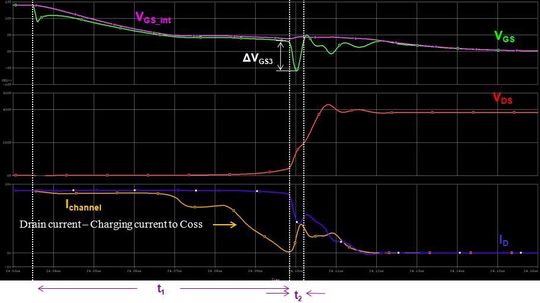
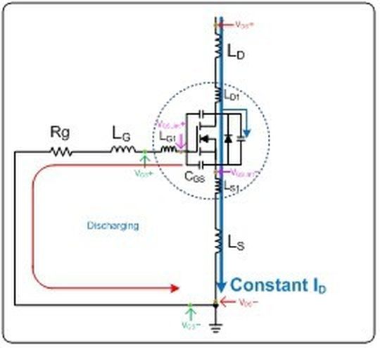
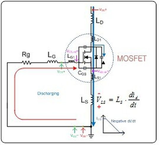
Figure 2 shows the PSPICE simulation waveforms of the gate-to-source voltage, VGS; the internal gate-to-source voltage, VGS_int; the drain-to-source voltage, VDS; the current channel of MOSFET, Ichannel; and the drain current, ID, in clamped inductive load switching circuit. To explain the effect of parasitic inductances of the power MOSFET, the turn-off transient is divided into two intervals (t1~t2). Figure 3 shows the MOSFET equivalent circuit including parasitic inductances.


During Time Interval t1: The voltage VGS decreases exponentially due to discharging of input capacitance, which the gate-to-source capacitance, CGS, and the gate-to-drain capacitance, CGD, via the gate resistance, Rg, as shown in Figure 3(a). When the gate voltage reaches the gate plateau voltage, the channel current in the MOSFET is reduced due to output characteristics in MOSFET, which is a characteristic curve between the gate voltage and drain current. At the same time, the output capacitance is charged up slowly.
During Time Interval t2: The Coss of the SJ MOSFET becomes strongly non-linear, these effects give an extremely fast dv/dt and di/dt, as shown in Figure 2. At the same time, the voltage drop across the common-source inductance LS is caused by negative drain current slope (-diD/dt). This voltage drop leads to negative gate voltage. Due to this effect, the discharged current flows in the opposite direction, as shown in Figure 3(b). In this time, this equivalent circuit can be expressed as R-L-C series resonance circuits.
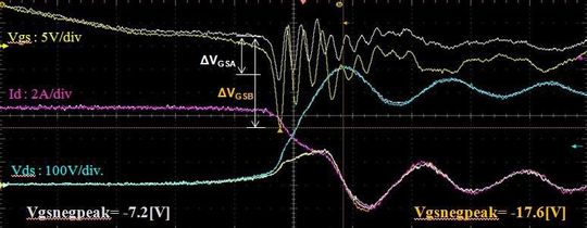
Two different values of gate inductance are compared in a clamped inductive load switching circuit. A circuit with a low value for LG has lower peak gate negative voltage (△VGSA). A circuit with a high LG value shows much higher peak gate negative voltage (△VGSB), as shown in Figure 4. To achieve optimized gate waveform, Designer should reduce gate inductance LG and common-source inductance LS.

(ID:42669669)


:quality(80)/p7i.vogel.de/wcms/46/7c/467c0afffbfd10c3553c2888a4a6289f/0130479810v3.jpeg)
:quality(80)/p7i.vogel.de/wcms/12/3d/123d9eb2c2e4ce13296371a2ad3718a4/0130412664v2.jpeg)
:quality(80)/p7i.vogel.de/wcms/d8/78/d878b7bfc23826e6ddfce42443836d28/0130384280v2.jpeg)
:quality(80)/p7i.vogel.de/wcms/13/20/13208d1c2797edd67d9ff216b403726b/0130471595v3.jpeg)
:quality(80)/p7i.vogel.de/wcms/38/cb/38cbe19e814dd30b94780bc3946547ab/0130446533v2.jpeg)
:quality(80)/p7i.vogel.de/wcms/a3/3e/a33e6d8a927d539ec6c3a0537f48f0f1/0130440028v2.jpeg)
:quality(80)/p7i.vogel.de/wcms/6b/61/6b61373f1c3f06f7f9343e6b0f0e9cc8/0130225062v1.jpeg)
:quality(80)/p7i.vogel.de/wcms/15/93/1593dd152e6d58c5fc5da0d331777c54/0130357398v2.jpeg)
:quality(80)/p7i.vogel.de/wcms/c2/88/c28805ea7b2261235475146a5b0c61f8/0130313028v2.jpeg)
:quality(80)/p7i.vogel.de/wcms/fa/8d/fa8dedee195f29c33c89d86311c258ee/0130104146v2.jpeg)
:quality(80)/p7i.vogel.de/wcms/cc/13/cc1378375499a26b5ddbb309d2155acb/0130085649v2.jpeg)
:quality(80)/p7i.vogel.de/wcms/6d/91/6d91abfa1b16ffcf470c7147facd7aa8/0130387695v2.jpeg)
:quality(80)/p7i.vogel.de/wcms/85/b0/85b0b32128f6d1968e975043f1e0b67b/0130342166v3.jpeg)
:quality(80)/p7i.vogel.de/wcms/1a/53/1a539631c940d184689460600bd2b395/0130410666v2.jpeg)
:quality(80)/p7i.vogel.de/wcms/10/45/1045969e69a1db4aaa73d0f74f55cc02/0129962687v2.jpeg)
:quality(80)/p7i.vogel.de/wcms/cd/32/cd3243e4a9a6476265ef6ea9463dfbd8/0129852659v2.jpeg)
:quality(80)/p7i.vogel.de/wcms/c7/f6/c7f61d0437c7f8fca3c6ff947ba2ad62/0129322490v2.jpeg)
:quality(80)/p7i.vogel.de/wcms/ba/e4/bae4e54395e5a53088060531ef99b814/0130359274v2.jpeg)
:quality(80)/p7i.vogel.de/wcms/35/af/35af7dd326d198475d06fbb69aa600b5/0130175971v2.jpeg)
:quality(80)/p7i.vogel.de/wcms/c0/2e/c02e7bf72bfc434888c37100e2511681/0130127767v3.jpeg)
:quality(80)/p7i.vogel.de/wcms/7c/04/7c04916c305164fb10bc6cb05b51d934/0130431065v2.jpeg)
:quality(80)/p7i.vogel.de/wcms/64/e5/64e5e333492f182ab7df5ab4c2b54c1e/0130463252v2.jpeg)
:quality(80)/p7i.vogel.de/wcms/0a/95/0a95db4508128c4e11d5d268bf2c0a77/0130440053v2.jpeg)
:quality(80)/p7i.vogel.de/wcms/b3/65/b365dd5433c8b6d36c56c92b72f5b368/0130401081v2.jpeg)
:quality(80)/p7i.vogel.de/wcms/85/c0/85c0cdd8fd326013aed52ca96777c998/0130426877v2.jpeg)
:quality(80)/p7i.vogel.de/wcms/f0/78/f07826d6c4e995980f1ada3377416aac/0130403626v4.jpeg)
:quality(80)/p7i.vogel.de/wcms/b6/c8/b6c8f7732da417bda3d298412f4c0ed8/0130453104v2.jpeg)
:quality(80)/p7i.vogel.de/wcms/47/ce/47ce64bad7990f276f68cbb24505f6dd/0130472850v2.jpeg)
:quality(80)/p7i.vogel.de/wcms/15/56/15564dea31861c376a385658c3b961a3/0130465243v2.jpeg)
:quality(80)/p7i.vogel.de/wcms/98/ad/98ad595a6372aae8dbeac71681d23f41/0130450258v2.jpeg)
:quality(80)/p7i.vogel.de/wcms/bf/2a/bf2aad428ab1a80e6738fdbdc2efeb7e/0130453420v2.jpeg)
:quality(80)/p7i.vogel.de/wcms/d6/ea/d6eac438c362c545cab42ef0f30bcfc0/0130136975v2.jpeg)
:quality(80)/p7i.vogel.de/wcms/e5/6c/e56ceb935ba09cb66a4fd0f961b2d3e9/0129642888v2.jpeg)
:quality(80)/p7i.vogel.de/wcms/69/1f/691f39ba12be3cad90eb88bdabc456a6/0127321404v2.jpeg)
:fill(fff,0)/images.vogel.de/vogelonline/companyimg/130400/130457/65.jpg)
:quality(80)/p7i.vogel.de/wcms/da/e4/dae45caa7f4fa7125e17b07d9da016bb/0125786170v2.jpeg)
:quality(80)/p7i.vogel.de/wcms/3f/45/3f45b76aef06121a2016dd70cbecd5f3/0127037255v2.jpeg)