
:quality(80)/p7i.vogel.de/wcms/95/83/95831d622af8fe99f4d14a3a3311d509/0131356667v3.jpeg "Funktionierendes Qubit-Array mit Abständen zwischen den Plunger- (P) und Barriere- (B) Gates von knapp 6 Nanometern, ermöglicht durch High-NA-EUV-Lithografie. Das Bild zeigt außerdem die Akkumulations- (A) und Einschluss- (C) Gates. (Bild: Imec)")
:quality(80)/p7i.vogel.de/wcms/9f/13/9f13686bb894142875a93de7f6c3aabe/0131278942v2.jpeg "Hoher Druck:
Die Luft- und Raumfahrtbranche muss schneller entwickeln, effizienter planen und Ressourcen besser nutzen. Hierbei kann Quantencomputing helfen. (Bild: Romolo Tavani | Adobe Stock)")
:quality(80)/p7i.vogel.de/wcms/e1/9c/e19ca48e7ee7b6604240bdb1a02a3a7d/0131251245v2.jpeg "„Fühlender Muskel“: Feine, hell schimmernde Kanäle aus flüssigem Metall in einem Serpentinenmuster fungieren gleichzeitig als elektrische Heizung und hochsensible Dehnungssensoren. (Bild: Gemini / KI-generiert)")
:quality(80)/p7i.vogel.de/wcms/67/81/67811b3e2ec01ebfe19b7febbb21893a/0131397616v2.jpeg "Europa will mit DARE SGA1 eine eigene Supercomputing-Infrastruktur auf Basis offener RISC-V-Technologie aufbauen. Chiplets, Software-Stack und parallele Debugging-Werkzeuge sollen technologische Souveränität und Exascale-Leistung für Forschung, Industrie und KI ermöglichen. (Bild: Dall-E / KI-generiert)")
:quality(80)/p7i.vogel.de/wcms/f5/d8/f5d88603ca3a0e39de02cfd582a170be/0131421069v2.jpeg "Perowskit-Photovoltaik industriell fertigen: Forschende entwickeln skalierbares Verfahren. (Bild: Alexander Diercks, KIT)")
:quality(80)/p7i.vogel.de/wcms/c2/b9/c2b94412f90cbea098c5b0a49e93e3f7/0131368512v2.jpeg "Crescendo-Plattform von Empower Semiconductor für „Vertical Power Delivery“ (VPD). Laut Angaben der Nachrichtenagentur Bloomberg und Reuters ist Analog Devices an einer Übernahme des Herstellers von Power Management Chips für KI-Lasten in Rechenzentren interessiert. (Bild: Empower Semiconductor)")
:quality(80)/p7i.vogel.de/wcms/17/71/1771c0b139e32eced60c0f60abd045dc/0131202175v2.jpeg "Chinas bekanntestes KI-Modell von Deepseek will sich von der Nvidia-Abhängigkeit freischwimmen. Die Verantwortlichen haben erste Schritte unternommen. (Bild: Dall-E / KI-generiert)")
:quality(80)/p7i.vogel.de/wcms/ab/6e/ab6ee4358adb3ef565a3af4e923dae6b/0131202314v2.jpeg "Wiederbelebung der Partnerschaft: Apple plant offenbar die Produktion künftiger Prozessoren in US-Werken von Intel. (Bild: Intel Corp.)")
:quality(80)/p7i.vogel.de/wcms/cc/88/cc885723ea62775c0f7a0c72fc63fbac/0131381195v2.jpeg "Enorme Durchdringung: Dank der hohen Reichweite der LoRaWAN-Technologie lassen sich auch weitläufige und metallisch stark verbaute Prozessanlagen kosteneffizient und komplett kabellos überwachen. (Bild: Wika)")
:quality(80)/p7i.vogel.de/wcms/4e/a8/4ea857349b0630ab44c1ed52a2b8ea67/0131332364v2.jpeg "Controlmaster 1721 von ICO: 19-Zoll-Industrie-PC in 4HE-Bauhöhe (Bild: ICO)")
:quality(80)/p7i.vogel.de/wcms/5b/f2/5bf2fc2e46775b70614326a4003940ea/0131238162v2.jpeg "Das Thema Batterierecycling nimmt in Europa an Fahrt auf. Das zeigt sich unter anderem bei den Patenten im Batterierecycling. (Bild: Gemini / KI-generiert)")
:quality(80)/p7i.vogel.de/wcms/2e/78/2e789ef76c84f5fcdf02b5697a22f9ab/0131062677v2.jpeg "Zur Stärkung des Portfolios insbesondere mit Blick auf Edge-Cloud-Infrastruktur für KI-Lösungen übernimmt Low-Power-FPGA-Spezialist Lattice Semiconductor den Firmware- und Cloud-Software-Entwickler AMI. (Bild: Lattice)")
:quality(80)/p7i.vogel.de/wcms/d4/1d/d41d81ec84a42b4fd5d732d36d0021ce/0130877962v2.jpeg "Im Element:
Auch fast 40 Jahre, nachdem sich der Elektrotechnik-Ingenieur als Berater für ASIC- und FPGA-Entwicklung selbstständig machte, hält Eugen Krassin immer noch Schulungen und Seminare zur programmierbaren Logik. (Bild: Toby Giessen)")
:quality(80)/p7i.vogel.de/wcms/9c/79/9c798ab2b4c18ba0a2c24f2491798d36/0130550888v2.jpeg "Prof. Dr. Christian Siemers ist Hochschullehrer und Autor: „Zeitlos geblieben ist der Wille, die entwickelten Systeme wirklich verstehen zu wollen.“ (Bild: TU Clausthal)")
:quality(80)/p7i.vogel.de/wcms/b6/e7/b6e755d9e704319c0bb59dc1ac2d67e8/0130537290v2.jpeg "Menschliches Wissen, künstliche Intelligenz: Intelligente Datenverarbeitung direkt am Einsatzort verlangt nach dem Zusammenspiel von KI, Hardware-Know-how und konkreter Anwendungserfahrung. (Bild: Dall-E / KI-generiert)")
:quality(80)/p7i.vogel.de/wcms/67/56/675687b9430f1ca7d89ee078f527984d/0131408598v2.jpeg "BSI veröffentlicht G7-Richtlinie zu Software Bill of Materials for AI. (Bild: BSI)")
:quality(80)/p7i.vogel.de/wcms/a9/3f/a93f4dac41be6ba50eb634f5e4e7f7b7/0131355751v2.jpeg "Das Programm soll vereinfachten Zugang zu moderner EDA-Software (Electronic Design Automation) für kleinere Unternehmen, Start-ups und Forschungseinrichtungen bieten. (Bild: Siemens EDA)")
:quality(80)/p7i.vogel.de/wcms/aa/79/aa79a807ba1ce61e6656226679e05f9c/0131288690v2.jpeg "(Bild: KiCad)")
:quality(80)/p7i.vogel.de/wcms/35/c2/35c2b1da065361aefeea668c786531c9/0131280558v2.jpeg "Im Fokus des neuen Labors: Mit den Testsystemen von Keysight stellen Entwickler die Interoperabilität von Ladesystemen über verschiedene regionale Normen wie CCS hinweg sicher. (Bild: Keysight)")
:quality(80)/p7i.vogel.de/wcms/05/83/0583267ea76f0beb94c4acef52d485e1/0130855074v2.jpeg "Arbiträrgenerator mit Direct Digital Synthesis (DDS): Wer komplexe Signalformen erzeugen will, musste sich in der Hardware-Anschaffung oft entscheiden. Durch eine clevere Firmware-Architektur verschmelzen nun beide Messtechnik-Welten in einem Gerät. (Bild: Spectrum Instrumentation)")
:quality(80)/p7i.vogel.de/wcms/b5/54/b5548923d20a751319550a3eb159af21/0131159519v2.jpeg "Die Nahfeldmessung eignet sich auch zur Charakterisierung großer Antennen-Arrays. Im Bild ist eine ESA-Antenne von Greenerwave zu sehen, die mithilfe des R&S TS8991-Antennentestsystems untersucht wird. (Bild: Rohde & Schwarz)")
:quality(80)/p7i.vogel.de/wcms/87/b6/87b60368567da3c6b65107c55f5f69ec/0130689118v2.jpeg "Messtechnik und Inspektion: In den vergangenen vier Jahrzehnten führte die Weiterentwicklung der Logiktechnologie-Roadmap zu einer Diversifizierung der Mess- und Inspektionswerkzeuge in den Fertigungsanlagen. (Bild: imec)")
:quality(80)/p7i.vogel.de/wcms/40/00/4000cee04363c2ad502a5cfadded2e0e/0131287222v2.jpeg "AMD Ryzen Pro 9000: Der Hersteller integriert erstmals die 3D-V-Cache-Technologie in Prozessoren für professionelle Workstations. (Bild: AMD)")
:quality(80)/p7i.vogel.de/wcms/7d/5b/7d5bd7b3575dd8745fac17cf8619a7c2/0131253052v3.jpeg "Fruitcore Robotics: Mit der Plattform Plexa One hält ein humanoider Roboter Einzug in die industrielle Fertigung. (Bild: Fruitcore Robotics)")
:quality(80)/p7i.vogel.de/wcms/67/dd/67dd59d72b9cc1c0128c2873419738d4/0131406116v2.jpeg "Der „State of Smart Manufacturing Report“ wurde zum elften Mal von Rockwell Automation veröffentlicht. (Bild: Rockwell Automation)")
:quality(80)/p7i.vogel.de/wcms/48/51/48516b200b1181bdca44488163b1aeb7/0131056202v2.jpeg "Stilisierte Produktionslinie mit markierten Einsatzpunkten für KI – etwa in Monitoring, virtuellen Sensoren und Prozessregelung (Symbolbild). (Bild: Dall-E / KI-generiert)")
:quality(80)/p7i.vogel.de/wcms/cf/8a/cf8af11d7828bc29be5e28a4e2a8367e/0131438113v2.jpeg "Zhou Qunfei hat ein Produkt, an dem in der Vergangenheit Smartphone-Anbieter interessiert waren. Jetzt sollen die Lösungen auch andere Bereiche erobern. (Bild: Dall-E / KI-generiert)")
:quality(80)/p7i.vogel.de/wcms/01/ef/01ef061683055328c66929c3abd3772a/0131410387v2.jpeg "Bei Samsung stehen alle Zeichen auf Streik in den südkoreanischen Werken (Symbolbild). (Bild: Dall-E / KI-generiert)")
:quality(80)/p7i.vogel.de/wcms/d6/ea/d6eac438c362c545cab42ef0f30bcfc0/0130136975v2.jpeg "Die Bewerbungsphase für den James Dyson Award 2026 ist gestartet. (Bild: Dyson)")
:quality(80)/p7i.vogel.de/wcms/e5/6c/e56ceb935ba09cb66a4fd0f961b2d3e9/0129642888v2.jpeg "(Bild: Vogel Professional Education)")
:quality(80)/p7i.vogel.de/wcms/69/1f/691f39ba12be3cad90eb88bdabc456a6/0127321404v2.jpeg "Das Kreativteam Christian Göller, GreatScott! und Christopher Becht (v. l. n. r.): erfolgreiches Creator-Marketing im B2B-Sektor (Bild: Würth Elektronik)")
Anbieter zum Thema
:fill(fff,0)/images.vogel.de/vogelonline/companyimg/130400/130457/65.jpg "mev_logo-RGB-L.jpg ()")
External Parasitic Coupling Drain-Source Capacitances
 MOSFET Equivalent, Including Parasitic Coupling Capacitance")
External coupling Cgd is one of the root causes for ringing affected by the device and PCB layout. Figure 5 shows the MOSFET equivalent circuit, including resonant circuit with coupling gate-drain capacitance. External gate-drain capacitance is coupled through parasitic inductances, leading to resonance, causing gate oscillation with gate and drain inductance when MOSFET switching speed is fast. It could lead to the gate oscillation at turn-on and turn-off, destruction of gate oxide, or out–of-control or poor EMI performance. External coupling Cgd must be reduced as much as possible to reduce gate oscillation. The capacity between traces can be calculated by Equation (2):
 Single Layer: Layout Example with Increased External Cgd")
 Double-Layer: Layout Example with Increased External Cgd")
 and 7b) Layout Example with reduced External Cgd")
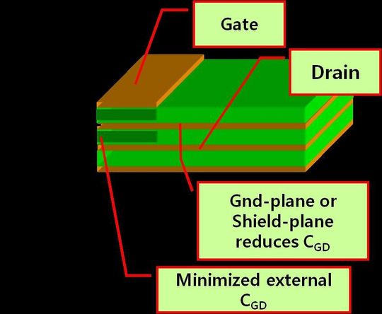
Figure 6 shows layout examples with high external Cgd and figure 7 shows layout solutions with reduced external Cgd. The difference in oscillations is shown in Figure 8. VGS (green line) and VDS (magenta line) are during turn off. The experimental waveforms show the effect of the high and low external Cgd in a given layout. The oscillation effect can be forced by increasing the output power level or decreasing the input voltage at the same output power. This can also occur after an AC line drop out: when line voltage is back, the boost stage charges up the bulk capacitor to nominal voltage.
 Turn-Off Waveforms by Different External Cgd")
 Turn-Off Waveforms by Different External Cgd")
During the time when the MOSFET turns off, the drain current is quite high. The drain current commutates to the output capacitance, Coss, of the MOSFET and charges it up to DC bus voltage. The voltage slope is proportional to the load current and inversely proportional to the value of the output capacitance. The value of Coss is high at low VDS and low at high VDS. As a result, dv/dt values of drain-source voltage change during turn-off. The high dv/dt values lead to capacitive displacement currents due to all the parasitic capacitances.
Conclusion: The faster switching of the power MOSFETs enable higher power conversion efficiency. However, parasitic components in the devices and boards are involving switching characteristics more as the switching speed is getting faster. This creates unwanted side effects, like high voltage or current spikes or poor EMI performance. To achieve balance, it is important to optimize gate drive circuitry and minimize parasitic inductances and capacitances on PCB board.
(ID:42669669)
:quality(80)/p7i.vogel.de/wcms/da/e4/dae45caa7f4fa7125e17b07d9da016bb/0125786170v2.jpeg "Soft termination prevents cracks by absorbing mechanical stress through a resin layer. (Bild: TAIYO YUDEN CO., LTD.)")
:quality(80)/p7i.vogel.de/wcms/3f/45/3f45b76aef06121a2016dd70cbecd5f3/0127037255v2.jpeg "Piezoelectric actuators turn flat car displays into responsive surfaces, providing tactile and acoustic feedback for safer, more intuitive interaction. (Bild: TAIYO YUDEN CO., LTD.)")