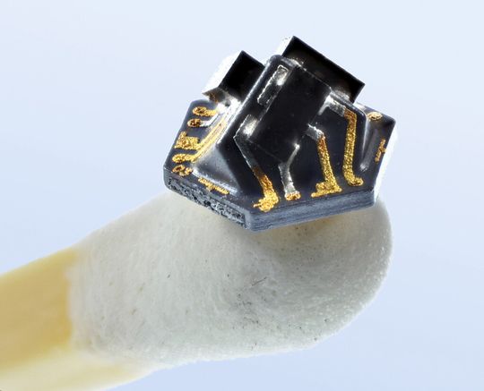
MID technology exemplified by magnetic field sensors
It is the possibility of combining the freedom of 3D shaping provided by injection molding technology with the integration of many possible functions; this is both unique and convincing.
Anbieter zum Thema

Today 3D Molded Interconnect Devices (3D-MID) can be found as part of many systems although it might not be obvious on the first glance. MID technology provides the creative designer with a tool for e.g. using the small space given in mobile devices in an optimal way, so that both miniaturization and performance can be improved.
An MID for a fluidic sensor system can be not only housing but also a highly flexible electrical interposer and fluidic interface. By using almost all surfaces of modules for an interactive Braille display with touch functionality a display can be designed that opens a whole new door for blind people to access the internet and state of the art software.
So is MID technology the right choice for my new product? Often you can answer this question with yes, if miniaturization, integration of additional functionality, optimizing the given space or 3D arrangement of different elements are an important issue for the application. Depending on the individual demands of your product, laser direct structuring using LPKF-LDS-technology or other MID methods will be the appropriate manufacturing technology for your new 3-dimensional system carrier.
Laser direct structuring of devices with complex shapes
There are a lot of thermoplastics suitable for the LPKF-LDS-technology commercially available. So, one will always find the proper material for different needs of different applications. An LDS thermoplastic contains special laseractivatable fillers so that the surfaces of an injection molded part can be selectively activated by laser-radiation and afterwards metalized by electro less plating. A common metal layer system is copper, nickel and flash gold which is well known in PCB production as well, but also other finishes are possible.

Due to the 3D-capability of the laser-process even devices with complex shapes can be machined. Because only the activated areas of the plastic part are metalized, the additive processing consumes only a minimal amount of material, a good thing from both the economical and the ecological point of view. The schematic view in figure 1 illustrates the short process chain and the simplicity of laserdirectstrucuring.
In the following two different magnetic sensor systems will serve as examples to show the possibilities and advantages of MID technology for applications. Measuring and analyzing a magnetic field is a complex task for metrology. The magnetic field possesses not only field strength and a direction in every spot, but since it is almost never homogeneous there is also a gradient to be detected. But especially that spatial characteristic makes MID technology the perfect tool. In the funded project Adima-3D (IGF Vorhaben 17163 N) two different magnetic sensor systems, with high demand for accuracy and stability have been set up at HSG-IMAT.
(ID:42360897)


:quality(80)/p7i.vogel.de/wcms/46/7c/467c0afffbfd10c3553c2888a4a6289f/0130479810v3.jpeg)
:quality(80)/p7i.vogel.de/wcms/12/3d/123d9eb2c2e4ce13296371a2ad3718a4/0130412664v2.jpeg)
:quality(80)/p7i.vogel.de/wcms/d8/78/d878b7bfc23826e6ddfce42443836d28/0130384280v2.jpeg)
:quality(80)/p7i.vogel.de/wcms/13/20/13208d1c2797edd67d9ff216b403726b/0130471595v3.jpeg)
:quality(80)/p7i.vogel.de/wcms/38/cb/38cbe19e814dd30b94780bc3946547ab/0130446533v2.jpeg)
:quality(80)/p7i.vogel.de/wcms/a3/3e/a33e6d8a927d539ec6c3a0537f48f0f1/0130440028v2.jpeg)
:quality(80)/p7i.vogel.de/wcms/6b/61/6b61373f1c3f06f7f9343e6b0f0e9cc8/0130225062v1.jpeg)
:quality(80)/p7i.vogel.de/wcms/15/93/1593dd152e6d58c5fc5da0d331777c54/0130357398v2.jpeg)
:quality(80)/p7i.vogel.de/wcms/c2/88/c28805ea7b2261235475146a5b0c61f8/0130313028v2.jpeg)
:quality(80)/p7i.vogel.de/wcms/fa/8d/fa8dedee195f29c33c89d86311c258ee/0130104146v2.jpeg)
:quality(80)/p7i.vogel.de/wcms/cc/13/cc1378375499a26b5ddbb309d2155acb/0130085649v2.jpeg)
:quality(80)/p7i.vogel.de/wcms/6d/91/6d91abfa1b16ffcf470c7147facd7aa8/0130387695v2.jpeg)
:quality(80)/p7i.vogel.de/wcms/85/b0/85b0b32128f6d1968e975043f1e0b67b/0130342166v3.jpeg)
:quality(80)/p7i.vogel.de/wcms/1a/53/1a539631c940d184689460600bd2b395/0130410666v2.jpeg)
:quality(80)/p7i.vogel.de/wcms/10/45/1045969e69a1db4aaa73d0f74f55cc02/0129962687v2.jpeg)
:quality(80)/p7i.vogel.de/wcms/cd/32/cd3243e4a9a6476265ef6ea9463dfbd8/0129852659v2.jpeg)
:quality(80)/p7i.vogel.de/wcms/c7/f6/c7f61d0437c7f8fca3c6ff947ba2ad62/0129322490v2.jpeg)
:quality(80)/p7i.vogel.de/wcms/ba/e4/bae4e54395e5a53088060531ef99b814/0130359274v2.jpeg)
:quality(80)/p7i.vogel.de/wcms/35/af/35af7dd326d198475d06fbb69aa600b5/0130175971v2.jpeg)
:quality(80)/p7i.vogel.de/wcms/c0/2e/c02e7bf72bfc434888c37100e2511681/0130127767v3.jpeg)
:quality(80)/p7i.vogel.de/wcms/7c/04/7c04916c305164fb10bc6cb05b51d934/0130431065v2.jpeg)
:quality(80)/p7i.vogel.de/wcms/64/e5/64e5e333492f182ab7df5ab4c2b54c1e/0130463252v2.jpeg)
:quality(80)/p7i.vogel.de/wcms/0a/95/0a95db4508128c4e11d5d268bf2c0a77/0130440053v2.jpeg)
:quality(80)/p7i.vogel.de/wcms/b3/65/b365dd5433c8b6d36c56c92b72f5b368/0130401081v2.jpeg)
:quality(80)/p7i.vogel.de/wcms/85/c0/85c0cdd8fd326013aed52ca96777c998/0130426877v2.jpeg)
:quality(80)/p7i.vogel.de/wcms/f0/78/f07826d6c4e995980f1ada3377416aac/0130403626v4.jpeg)
:quality(80)/p7i.vogel.de/wcms/b6/c8/b6c8f7732da417bda3d298412f4c0ed8/0130453104v2.jpeg)
:quality(80)/p7i.vogel.de/wcms/47/ce/47ce64bad7990f276f68cbb24505f6dd/0130472850v2.jpeg)
:quality(80)/p7i.vogel.de/wcms/15/56/15564dea31861c376a385658c3b961a3/0130465243v2.jpeg)
:quality(80)/p7i.vogel.de/wcms/98/ad/98ad595a6372aae8dbeac71681d23f41/0130450258v2.jpeg)
:quality(80)/p7i.vogel.de/wcms/bf/2a/bf2aad428ab1a80e6738fdbdc2efeb7e/0130453420v2.jpeg)
:quality(80)/p7i.vogel.de/wcms/d6/ea/d6eac438c362c545cab42ef0f30bcfc0/0130136975v2.jpeg)
:quality(80)/p7i.vogel.de/wcms/e5/6c/e56ceb935ba09cb66a4fd0f961b2d3e9/0129642888v2.jpeg)
:quality(80)/p7i.vogel.de/wcms/69/1f/691f39ba12be3cad90eb88bdabc456a6/0127321404v2.jpeg)
:fill(fff,0)/p7i.vogel.de/companies/63/88/63887b860cf66/me-logo-400px.jpeg)
:fill(fff,0)/images.vogel.de/vogelonline/companyimg/130400/130457/65.jpg)
:quality(80)/p7i.vogel.de/wcms/ab/73/ab73d241611c109a242a4e5f1b50d01e/0128483827v4.jpeg)
:quality(80)/p7i.vogel.de/wcms/da/e4/dae45caa7f4fa7125e17b07d9da016bb/0125786170v2.jpeg)