Anbieter zum Thema
3D magnetic field sensor system with low-cost SMD sensors
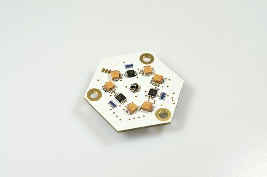
In this system three commercially available low-cost SMD magnetic field sensors are arranged perpendicularly, so that they build a three dimensional measuring system. The MID carrier is built in LPKF-LDS-technology. Therefore it is very easy to flexibly adjust the metallization layout at any time, e.g. to replace the SMD sensors by other magnet field sensors optimized for different field strength.

Today commercially available 3D magnetic field sensors usually do not have the same sensitivity in all three axes. This is different with the MID based system as there are three equal sensors with equal properties in use. The MID and the electrical layout is designed to position the SMD as close to each other as possible to detect the components of the field almost in one single spot.
A surrounding border underneath the SMD makes it possible for a vacuum tool of a state of the art assembly machine to handle the MID as an SMD itself. The MID is also designed with the highest amount of symmetry in order to minimize distortion or troublesome effects e.g. due to temperature changes. All this adds up to a very compact system with a volume of only 4 x 4 x 2.5 mm³.
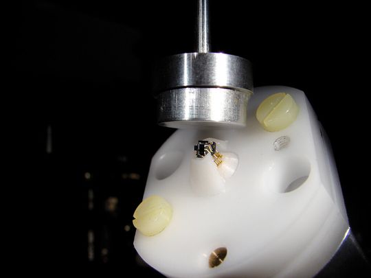
A challenge for manufacturing this system is the 3D assembly. On one hand the three magnetic field sensors have to be positioned accurately in 90° to each other, on the other hand there is a need for an automated process with short cycle time in order to maintain the advantage of using low-cost SMD-sensors.
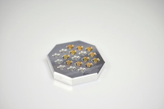
The key to achieve this goal is to use multiple work piece holders in a multi axis substrate manipulating device. Depending on the working area of the assembly machine the time needed for loading and unloading and for positioning the devices can be reduced highly. The multiple work piece holder in figure 4 can carry up to 19 MID modules and can be positioned in the correct angles in a very accurate way.

The same assembly machine can be used for characterizing the system. Therefore the MID is mounted onto a special interface for electrical connection and the interface can be assembled onto the multi axis substrate manipulating device instead of a multiple work piece carrier. A permanent magnet and the MID modules can now be arranged in relative position to each other with the same high accuracy like the previous assembly.
Measuring the gradient and eliminating interfering fields
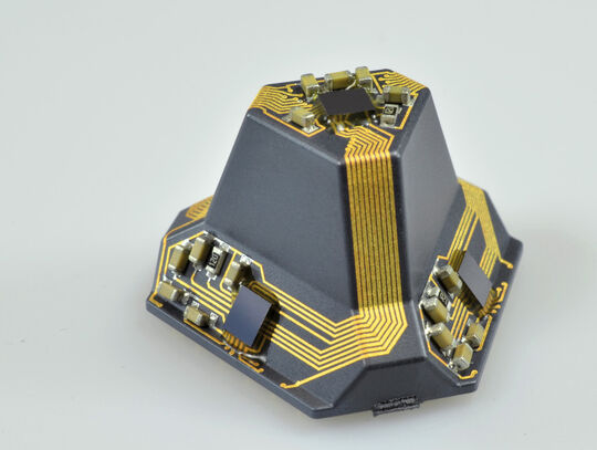
The second MID based magnetic field sensor system can detect the gradient of the field within a small volume. Therefore magnetic field sensor chips are used that are capable of measuring three dimensionally themselves. Four of them are positioned in a way that they lie on the edges of a virtual pyramid made of equilateral triangles. By differential calculation the field gradient for each axis can be detected.

A system like this is able to find out the position and direction of a known field even if other magnetic fields may interfere. That is a big benefit e.g. when using a permanent magnet as a positioning sensor in an electric motor. But also in this case the single sensor chips do not have equal sensitivity in all axes that is why they are positioned within defined angles in order to compensate this effect a bit.
Precision plays an important role for this system. That is why flip chip assembly using non conductive adhesive (NCA) is used. The NCA is dispensed to the substrate in the first step. The chips have Au studs as bumps and are pressed to the substrate with defined pressure and a heated tool. By that the NCA is cured within seconds creating a reliable electrical and mechanical connection. As the sensor chip is fixed in position through the curing process a very high accuracy even after assembly can be achieved. The necessary passive SMDs can be mounted by means of leadless soldering right next to the chip. A peripheral microcontroller unit on the PCB completes the system. The MID sensor system can be mounted as an SMD on the PCB as well. Molded MID bumps on the backside ensure reliable connections.

New applications with MID technology
The two magnetic field sensor systems introduced above are results of a funded research project and therefore no commercially available products. But they form the basis for a product development and what is more important; they demonstrate the possibilities of MID technology when complex requirements are met by creative and innovative ideas.
Today as well as in the future MID technology will especially be able to create a new solution, if miniaturized products are capable of using spatial design and 3D assembly of functional components. Current activities with focus on new and improved materials with increased thermal conductivity and robust mechanical properties will open MID for new applications, e.g. for LED lighting solutions.
For more than 15 years HSG-IMAT is doing R&D in the field of polymer based Microsystems. For almost 2 years the TransferFab also provides the infrastructure for accompanying our customers on the whole path from the idea to prototypes or even small series.
We gratefully thank the Federal Ministry of Economics and Technology for funding this project 17163N within the program for promotion of industrial collective research (IGF).
* Dr. Ulrich Keßler is head of micro assembly at the Hahn-Schickard institute für microassembly technology (HSG-IMAT)
(ID:42360897)


:quality(80)/p7i.vogel.de/wcms/46/7c/467c0afffbfd10c3553c2888a4a6289f/0130479810v3.jpeg)
:quality(80)/p7i.vogel.de/wcms/12/3d/123d9eb2c2e4ce13296371a2ad3718a4/0130412664v2.jpeg)
:quality(80)/p7i.vogel.de/wcms/d8/78/d878b7bfc23826e6ddfce42443836d28/0130384280v2.jpeg)
:quality(80)/p7i.vogel.de/wcms/13/20/13208d1c2797edd67d9ff216b403726b/0130471595v3.jpeg)
:quality(80)/p7i.vogel.de/wcms/38/cb/38cbe19e814dd30b94780bc3946547ab/0130446533v2.jpeg)
:quality(80)/p7i.vogel.de/wcms/a3/3e/a33e6d8a927d539ec6c3a0537f48f0f1/0130440028v2.jpeg)
:quality(80)/p7i.vogel.de/wcms/6b/61/6b61373f1c3f06f7f9343e6b0f0e9cc8/0130225062v1.jpeg)
:quality(80)/p7i.vogel.de/wcms/15/93/1593dd152e6d58c5fc5da0d331777c54/0130357398v2.jpeg)
:quality(80)/p7i.vogel.de/wcms/c2/88/c28805ea7b2261235475146a5b0c61f8/0130313028v2.jpeg)
:quality(80)/p7i.vogel.de/wcms/fa/8d/fa8dedee195f29c33c89d86311c258ee/0130104146v2.jpeg)
:quality(80)/p7i.vogel.de/wcms/cc/13/cc1378375499a26b5ddbb309d2155acb/0130085649v2.jpeg)
:quality(80)/p7i.vogel.de/wcms/6d/91/6d91abfa1b16ffcf470c7147facd7aa8/0130387695v2.jpeg)
:quality(80)/p7i.vogel.de/wcms/85/b0/85b0b32128f6d1968e975043f1e0b67b/0130342166v3.jpeg)
:quality(80)/p7i.vogel.de/wcms/1a/53/1a539631c940d184689460600bd2b395/0130410666v2.jpeg)
:quality(80)/p7i.vogel.de/wcms/10/45/1045969e69a1db4aaa73d0f74f55cc02/0129962687v2.jpeg)
:quality(80)/p7i.vogel.de/wcms/cd/32/cd3243e4a9a6476265ef6ea9463dfbd8/0129852659v2.jpeg)
:quality(80)/p7i.vogel.de/wcms/c7/f6/c7f61d0437c7f8fca3c6ff947ba2ad62/0129322490v2.jpeg)
:quality(80)/p7i.vogel.de/wcms/ba/e4/bae4e54395e5a53088060531ef99b814/0130359274v2.jpeg)
:quality(80)/p7i.vogel.de/wcms/35/af/35af7dd326d198475d06fbb69aa600b5/0130175971v2.jpeg)
:quality(80)/p7i.vogel.de/wcms/c0/2e/c02e7bf72bfc434888c37100e2511681/0130127767v3.jpeg)
:quality(80)/p7i.vogel.de/wcms/7c/04/7c04916c305164fb10bc6cb05b51d934/0130431065v2.jpeg)
:quality(80)/p7i.vogel.de/wcms/64/e5/64e5e333492f182ab7df5ab4c2b54c1e/0130463252v2.jpeg)
:quality(80)/p7i.vogel.de/wcms/0a/95/0a95db4508128c4e11d5d268bf2c0a77/0130440053v2.jpeg)
:quality(80)/p7i.vogel.de/wcms/b3/65/b365dd5433c8b6d36c56c92b72f5b368/0130401081v2.jpeg)
:quality(80)/p7i.vogel.de/wcms/85/c0/85c0cdd8fd326013aed52ca96777c998/0130426877v2.jpeg)
:quality(80)/p7i.vogel.de/wcms/f0/78/f07826d6c4e995980f1ada3377416aac/0130403626v4.jpeg)
:quality(80)/p7i.vogel.de/wcms/b6/c8/b6c8f7732da417bda3d298412f4c0ed8/0130453104v2.jpeg)
:quality(80)/p7i.vogel.de/wcms/47/ce/47ce64bad7990f276f68cbb24505f6dd/0130472850v2.jpeg)
:quality(80)/p7i.vogel.de/wcms/15/56/15564dea31861c376a385658c3b961a3/0130465243v2.jpeg)
:quality(80)/p7i.vogel.de/wcms/98/ad/98ad595a6372aae8dbeac71681d23f41/0130450258v2.jpeg)
:quality(80)/p7i.vogel.de/wcms/bf/2a/bf2aad428ab1a80e6738fdbdc2efeb7e/0130453420v2.jpeg)
:quality(80)/p7i.vogel.de/wcms/d6/ea/d6eac438c362c545cab42ef0f30bcfc0/0130136975v2.jpeg)
:quality(80)/p7i.vogel.de/wcms/e5/6c/e56ceb935ba09cb66a4fd0f961b2d3e9/0129642888v2.jpeg)
:quality(80)/p7i.vogel.de/wcms/69/1f/691f39ba12be3cad90eb88bdabc456a6/0127321404v2.jpeg)
:fill(fff,0)/p7i.vogel.de/companies/63/88/63887b860cf66/me-logo-400px.jpeg)
:fill(fff,0)/images.vogel.de/vogelonline/companyimg/130400/130457/65.jpg)
:quality(80)/p7i.vogel.de/wcms/ab/73/ab73d241611c109a242a4e5f1b50d01e/0128483827v4.jpeg)
:quality(80)/p7i.vogel.de/wcms/da/e4/dae45caa7f4fa7125e17b07d9da016bb/0125786170v2.jpeg)